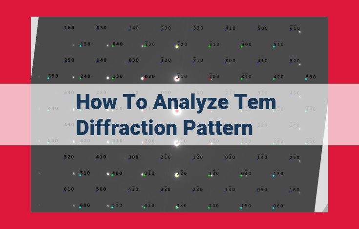
Analyzing TEM diffraction patterns involves interpreting the spot arrangement and intensities to determine crystallographic information. The pattern’s geometry yields unit cell parameters and crystal orientation, while spot intensities provide information on atomic positions and crystal structure. By measuring spot distances and angles, researchers can identify phases, determine preferred crystallographic orientations (texture), and analyze crystal lattice distortion. Advanced techniques like zonal analysis and image processing enhance data interpretation, allowing for detailed characterization of materials’ microstructures and properties.
Advanced Crystallography Methods for Materials Analysis: A Comprehensive Guide
In the realm of materials science, advanced crystallography methods serve as indispensable tools for unraveling the intricate details of materials, revealing their atomic structures and deciphering their properties. This comprehensive guide will delve into the nuances of crystallography, exploring the cutting-edge techniques that empower scientists to probe the world of materials at the atomic level.
Sample Collection and Preparation Techniques: Laying the Foundation
The initial step in crystallographic analysis is meticulously collecting and preparing samples that are representative of the material under investigation. These samples can come in diverse forms, ranging from thin films to bulk solids, each requiring specialized preparation techniques to ensure optimal results.
Firstly, it is essential to collect samples free from contaminants and defects. This may involve mechanical techniques such as cutting, grinding, or polishing to remove surface impurities or unwanted layers. For delicate materials, methods like focused ion beam (FIB) milling or chemical etching can be employed with precise control.
Next, samples are prepared to achieve the necessary thickness for optimal electron penetration during analysis. This is particularly crucial for transmission electron microscopy (TEM), which requires ultrathin specimens that allow the electron beam to pass through. Techniques like ion milling or ultramicrotomy are often utilized to achieve the desired sample thickness.
Finally, the prepared samples are mounted on special holders or grids to facilitate their examination under the electron microscope. Specialized holders may include heating or cooling stages for in-situ observations or environmental cells to conduct analysis under specific atmospheric conditions.
Unlocking Material Secrets: Advanced Crystallography Techniques
With meticulously prepared samples in hand, scientists embark on the fascinating journey of crystallographic analysis, employing a range of advanced techniques to unravel the mysteries of materials. These techniques provide invaluable information about the material’s crystal structure, phase composition, and atomic arrangement.
One cornerstone of crystallography is electron microscopy, a powerful technique that allows direct visualization of materials at nanometer-scale resolution. By bombarding samples with a focused electron beam, scientists can obtain detailed images that reveal the intricate arrangement of atoms within the material.
Transmission electron microscopy (TEM) and scanning electron microscopy (SEM) are two commonly used electron microscopy techniques. TEM provides high-resolution images of thin samples, enabling detailed studies of atomic structure and defects. SEM, on the other hand, offers three-dimensional information about the sample’s surface topography and morphology.
Another crucial aspect of crystallographic analysis involves interpreting diffraction patterns. When a beam of electrons interacts with a crystalline material, it undergoes diffraction, resulting in a pattern of spots or rings on a detector. These patterns provide insights into the crystal structure and orientation of the material, allowing scientists to identify different phases and determine their crystallographic parameters.
Advanced crystallography methods, with their ability to probe materials at the atomic level, empower scientists to gain unprecedented insights into the structure and properties of materials. These techniques pave the way for tailored material design, advanced device fabrication, and a deeper understanding of the materials that shape our world. As technology continues to advance, so too will the capabilities of crystallographic analysis, opening up new avenues for scientific exploration and technological breakthroughs.
Unraveling the Microscopic World: Advanced Electron Microscopy Methods
In the realm of materials analysis, crystallography reigns supreme, offering invaluable insights into the intricate structure and properties of materials. Among the advanced techniques employed in crystallography, electron microscopy takes center stage, providing unprecedented visualization and characterization capabilities.
Transmission Electron Microscopy (TEM): A Journey into the Nanoworld
TEM unveils the ultrastructure of materials at the atomic level. It bombards samples with highly focused electron beams that penetrate the specimen, generating detailed images of crystal lattices, atomic defects, and grain boundaries. TEM’s exceptional resolution allows scientists to explore the tiniest details, unraveling the secrets hidden deep within materials.
Scanning Electron Microscopy (SEM): Unveiling Surface Topography
SEM, on the other hand, provides a different perspective. It scans the surface of a sample with an electron beam, detecting backscattered or secondary electrons to create high-resolution images. SEM excels in revealing topography, morphology, and surface composition, providing valuable insights into material properties and failure mechanisms.
Combining Electron Microscopy Methods: A Synergistic Approach
Combining TEM and SEM offers a comprehensive analysis of materials. By correlating high-resolution lattice images from TEM with surface topography data from SEM, researchers gain unparalleled understanding of materials behavior. This synergistic approach enables the identification of defects, grain orientations, and chemical composition variations within complex materials systems.
Advanced electron microscopy techniques empower materials scientists with unprecedented characterization capabilities. TEM and SEM provide complementary perspectives, enabling the exploration of materials properties from the atomic scale to the surface morphology. By harnessing the power of electron microscopy, scientists unlock the secrets of materials design, development, and performance, paving the way for transformative innovations in various fields.
Transmission Electron Microscope (TEM)
Advanced Crystallography Methods for Materials Analysis: Unveiling the Intricacies of Matter
In the realm of materials science, understanding the crystalline structure of materials is crucial for deciphering their properties and performance. Advanced crystallography methods provide invaluable tools for unraveling the intricate world of crystallography.
Sample Preparation and Observation
Crystallographic analysis begins with meticulous sample preparation. This involves carefully collecting and preparing specimens to ensure optimal observation.
Transmission Electron Microscope (TEM)
The Transmission Electron Microscope (TEM) shines a beam of high-energy electrons through the sample, enabling ultra-high-resolution imaging of crystal structures at the atomic level.
- TEM’s Advantages:
- Reveals structural details on an atomic scale
- Identifies chemical composition and defects within crystals
- Various Applications:
- Characterizing nanomaterials
- Analyzing crystal defects and interfaces
- Studying biological and environmental samples
Diffraction Pattern Interpretation
The electrons diffracted by the crystal produce a characteristic pattern that holds vital information about the crystal’s structure. Expert interpretation of these patterns is key to unlocking the crystalline secrets.
Crystallographic Analysis
With the diffracted data in hand, scientists can delve into advanced crystallographic analysis.
Crystallographic Information:
* Determine unit cell parameters, which describe the size and shape of the crystal’s building blocks
* Identify atomic positions within the unit cell
Phase Identification:
* Determine the crystal’s phase structure, revealing its specific arrangement of atoms
* Analyze phase composition and coexistence, providing insights into material properties
Texture Analysis:
* Uncover the preferred crystallographic orientations within the material
* Determine the impact of processing and thermal history on material characteristics
Advanced Techniques
Modern crystallography extends beyond basic analysis, offering a range of sophisticated methods.
Zonal Analysis:
* Analyze crystallographic zones and orientations, providing detailed insights into crystal growth and crystallographic relationships
Strain Analysis:
* Measure crystal lattice distortion, revealing information about external forces and internal stresses
Software Advancements
Specialized software complements crystallographic techniques, enhancing data processing and interpretation.
Image Processing Software:
* Enhance, analyze, and interpret high-resolution TEM images
* Perform quantitative analysis to extract crystallographic information
Crystallography Software:
* Visualize diffraction patterns in an Ewald Sphere for comprehensive data evaluation
* Employ crystallographic calculations for precise analysis
Diffraction Grating
Diffraction gratings split light into different wavelengths, enabling precise diffraction analysis. This technique provides insights into the crystal’s atomic structure and electronic properties.
Advanced crystallography methods empower researchers to unravel the mysteries of materials at the atomic level. By combining sample preparation, electron microscopy, diffraction pattern interpretation, and sophisticated software, scientists can decode the crystalline composition and properties that govern materials’ behavior. This knowledge paves the way for optimizing material performance and designing materials for specific applications, revolutionizing industries and advancing scientific discovery.
Advanced Crystallography: Revolutionizing Materials Analysis
Scanning Electron Microscope (SEM): The Sharp Eye for Material Secrets
In the realm of material analysis, the Scanning Electron Microscope (SEM) serves as a powerful tool, unveiling the intricate details of materials at an ultra-microscopic level. This remarkable device bombards samples with a focused beam of electrons, generating a wealth of information that aids in understanding material properties, microstructure, and composition.
As the electrons interact with the sample, they trigger various responses, including the emission of secondary electrons. These secondary electrons carry valuable insights into the sample’s topography, providing high-resolutions images that reveal even the tiniest of surface features.
SEM: A Multifaceted Analytical Powerhouse
SEM’s versatility extends beyond surface imaging. It also enables energy-dispersive spectroscopy (EDS), a technique that uncovers the elemental composition of materials. This allows researchers to identify and map different elements within a sample, shedding light on its chemical makeup.
Furthermore, SEM can provide crystallographic information by analyzing the diffraction patterns generated by the electron beam. These patterns hold clues about the crystal structure and orientation, providing insights into the material’s atomic arrangement and preferred growth directions.
Exploring the World of Advanced SEM Techniques
Beyond these fundamental capabilities, SEM has evolved into a sophisticated tool with specialized techniques that enhance its analytical prowess:
- Electron Backscatter Diffraction (EBSD): This technique reveals the crystal orientation and grain structure of materials, providing valuable information about their deformation behavior and crystallographic texture.
- Focused Ion Beam (FIB): FIB utilizes a finely focused ion beam to modify samples with remarkable precision. This allows for the preparation of thin sections for TEM analysis or the creation of cross-sections to study material interfaces.
Advanced Crystallography Methods for Materials Analysis
Sample Preparation and Observation
Diffraction Pattern Interpretation
To analyze crystallographic information, diffraction patterns play a crucial role. When X-rays, electrons, or neutrons interact with a crystalline sample, they generate interference patterns. These patterns contain valuable information about the arrangement of atoms within the crystal.
Imagine shining a flashlight at a grid. As the light passes through the grid, it creates a regular pattern of bright and dark bands on a screen. Similarly, X-rays interact with the regular arrangement of atoms in a crystal, producing a diffraction pattern that resembles a grid-like structure.
Each diffraction spot in the pattern corresponds to a specific set of atomic planes within the crystal. The intensity of the spots and their spacing provide clues about the crystal’s unit cell parameters and atomic positions. By analyzing the diffraction pattern, scientists can determine the crystal’s structure and identify phase composition.
However, interpreting diffraction patterns can be a challenging task. Specialized software and expert knowledge are often required to extract accurate information from these patterns. Advanced techniques like 3D reconstruction and image processing further enhance the analysis, enabling scientists to visualize and understand complex crystal structures.
Advanced Crystallography Methods for Materials Analysis: Unraveling the Atomic Structure of Matter
Crystallography, a powerful technique in materials analysis, offers a window into the atomic world, providing invaluable insights into the structure and properties of materials. Advanced crystallographic methods provide even deeper insights, revealing the intricate details of materials at the atomic level.
Crystallographic Information: Unit Cell Parameters and Atomic Positions
At the heart of crystallography lies the concept of the crystal unit cell, the fundamental building block that repeats throughout a crystal. Advanced crystallographic methods can accurately determine the unit cell parameters, including its dimensions and shape. Armed with this knowledge, scientists can deduce the atomic positions within the unit cell, mapping out the crystal’s atomic arrangement. This information is crucial for understanding the material’s properties, such as its electronic behavior, mechanical strength, and thermal conductivity.
By precisely measuring the positions of atoms in the unit cell, scientists can distinguish between different phases of the same material. Each phase represents a unique arrangement of atoms, resulting in distinct properties. Phase identification is paramount in research and industry, enabling the development of tailored materials for specific applications.
Furthermore, crystallographic techniques enable the determination of texture, which refers to the preferred orientation of crystals within a material. Understanding texture is essential for optimizing materials performance, as it influences properties such as strength, toughness, and corrosion resistance. By identifying and controlling texture, scientists can engineer materials with the desired combination of properties.
Phase Identification: Phase Structure and Composition Analysis
Phase Identification: Unveiling the Secrets of Material Composition
In the realm of materials analysis, crystallographic methods shine as powerful tools for deciphering the hidden secrets of matter. Phase identification stands as a pivotal aspect of this endeavor, unraveling the intricate dance of elements and their structural arrangements.
When a beam of electrons or X-rays encounters a crystal, it scatters in a characteristic pattern, known as a diffraction pattern. This pattern holds a wealth of information about the crystal’s phase, which refers to its unique arrangement of atoms. By analyzing the diffraction pattern, scientists can determine not only the phase structure but also the composition of the material.
Imagine a crystal as a microscopic dance floor, where atoms waltz and twirl in a coordinated fashion. The phase structure defines the rules of this dance, determining the types of atoms involved and their geometric arrangement. By understanding the phase structure, scientists can gain insights into the material’s properties and behavior.
Furthermore, phase identification reveals the chemical composition of the material, providing a blueprint of the elements present and their relative proportions. This knowledge is crucial for tailoring materials with specific properties for diverse applications, from energy storage to biomedical implants.
The ability to identify phases is the cornerstone of advanced crystallographic methods. It empowers scientists to unravel the complexities of materials and design new materials with unprecedented properties, pushing the boundaries of innovation.
Advanced Crystallography: Unraveling the Secrets of Material Architecture
Texture Analysis: Unveiling the Crystallographic Tapestry of Materials
In the realm of materials science, texture analysis stands as a pivotal technique, shedding light on the preferred crystallographic orientation of grains within a material. This knowledge holds profound implications for understanding the material’s properties and predicting its performance under various conditions.
The orientation of individual grains within a material can significantly influence its mechanical strength, electrical conductivity, and other properties. Texture analysis allows scientists to map the spatial distribution of these orientations, revealing the crystalline fabric that underpins a material’s structure and functionality.
Various techniques, such as X-ray and electron diffraction, enable researchers to gather diffraction patterns that contain information about the relative orientations of grains within the sample. Sophisticated computer algorithms then decipher these patterns, providing detailed maps of the material’s texture.
Understanding texture is crucial in fields such as metallurgy, geology, and materials engineering. Tailoring the texture of materials can enhance their properties, making them more suitable for specific applications. For instance, in the development of stronger and lighter metals for aircraft, controlling crystallographic texture is a key factor in achieving optimal strength and durability.
Advanced Crystallography Techniques: Unlocking the Secrets of Materials
Crystallography, the study of the arrangement of atoms and molecules in crystals, is a powerful tool for understanding the structure and properties of materials. Advanced crystallography methods provide invaluable insights into the composition, orientation, and even strain within materials.
Sample Preparation and Observation
The first step in crystallographic analysis is meticulous sample preparation to obtain high-quality images. This involves carefully collecting and preparing the sample, ensuring its cleanliness and suitability for electron microscopy.
Electron microscopes, such as transmission electron microscopes (TEM) and scanning electron microscopes (SEM), allow direct visualization of crystal structures. These microscopes generate high-resolution images that reveal the arrangement of atoms and defects within the material.
Crystallographic Analysis
Once the sample has been observed, the crystallographic data is extracted from the images. This includes determining the unit cell parameters that describe the crystal’s shape and its atomic positions within the unit cell. This information enables the phase identification of the material, both in terms of its structure and chemical composition.
Advanced Techniques
Beyond the basics, advanced crystallography techniques provide even more detailed insights into materials:
Zonal Analysis: A Deeper Dive into Crystal Structures
Zonal analysis focuses on identifying crystallographic zones, which are groups of crystallographic directions that share common characteristics. By analyzing these zones, researchers can determine the orientation of the crystal and the presence of specific defects or features.
Other Advanced Techniques
- Strain Analysis: Measures the distortion of the crystal lattice to understand mechanical stresses or other internal forces.
- Image Processing Software: Enhances, analyzes, and interprets images, aiding in accurate data extraction.
- Ewald Sphere: A visual representation of diffraction patterns used to analyze and interpret crystallographic data.
- Diffraction Grating: Separates light into different wavelengths to facilitate diffraction analysis.
By employing these advanced techniques, researchers can gain a comprehensive understanding of the structure, composition, and behavior of materials, enabling them to optimize materials for specific applications and push the boundaries of materials science.
Advanced Crystallography Methods for Materials Analysis
2. Crystallographic Analysis
Strain Analysis: Measuring Crystal Lattice Distortion
Unveiling the Secrets of Material Behavior: Strain Analysis in Crystallography
In the intricate world of materials science, understanding the internal stresses and strains within crystals is crucial for unlocking their hidden potential and predicting their performance under various conditions. Advanced crystallographic techniques, such as strain analysis, provide a powerful tool for deciphering these subtle distortions, offering valuable insights into the mechanical properties, defects, and overall behavior of materials.
The Dance of Atoms: Measuring Crystal Lattice Distortion
Crystal lattice distortion arises when external forces or internal stresses cause the regular arrangement of atoms in a crystal to deviate from its perfect symmetry. Strain analysis quantifies these deviations, providing a snapshot of the internal forces acting within the material. By employing advanced crystallographic techniques, researchers can precisely measure the displacement of atoms from their ideal positions, unraveling the complex interplay of forces that shape material behavior.
From Fractures to Failures: Predicting Material Performance
Strain analysis plays a pivotal role in predicting the performance of materials under various conditions. Excessive strain can lead to fractures, cracks, and other forms of material failure. By identifying areas of high strain or stress concentration, scientists can anticipate potential failure points and design materials with improved durability and resilience. This knowledge is indispensable for industries ranging from aerospace to automotive, where safety and reliability are paramount.
Harnessing the Power of Crystallography for Innovation
Strain analysis in crystallography not only enhances our fundamental understanding of materials but also drives innovation by enabling the development of advanced materials with tailored properties. By harnessing the power of these techniques, researchers can fine-tune the mechanical properties, optimize performance, and unlock new applications for materials in various fields.
Advanced Crystallography Methods for Materials Analysis
Crystallography plays a pivotal role in materials analysis, unraveling the atomic structure and properties of various materials. This blog post delves into advanced crystallography techniques that provide in-depth insights into materials’ characteristics.
Sample Preparation and Observation
The foundation of crystallographic analysis lies in sample preparation and observation. Electron microscopes, such as Transmission Electron Microscopes (TEM) and Scanning Electron Microscopes (SEM), provide magnified views of materials, enabling the examination of their surface morphology and internal structures.
Crystallographic Analysis
Once samples are prepared, crystallographic analysis techniques extract valuable information. These methods determine Crystallographic Information, including Unit Cell Parameters and Atomic Positions. They also identify Phase Structure and Composition and analyze Texture (preferred crystallographic orientation).
Advanced Techniques
For more detailed analysis, advanced techniques bring additional capabilities:
- Zonal Analysis: Delves into the geometry of crystals, analyzing crystallographic Zones and their Orientations.
- Strain Analysis: Measures Crystal Lattice Distortion, providing insights into mechanical properties.
- Image Processing Software: Enhances, analyzes, and interprets images obtained from electron microscopes, facilitating data extraction.
Image Processing Software: Empowering Image Analysis
Image processing software is indispensable for crystallography. It can:
- Enhance: Adjust contrast and brightness to improve image clarity.
- Analyze: Perform automated measurements and calculations on images.
- Interpret: Assist in identifying features and patterns, guiding subsequent analysis.
Ewald Sphere and Diffraction Grating
- Ewald Sphere: Visualizes Diffraction Patterns, aiding in data interpretation.
- Diffraction Grating: Splits light into different wavelengths, enabling Diffraction Analysis.
Advanced crystallography methods empower materials scientists with a comprehensive understanding of materials’ structure and properties. These techniques provide valuable insights into crystallographic information, phase structure, texture, and more. By leveraging these techniques, researchers can tailor materials for specific applications, advancing materials science and technology.
Crystallography Software:
- Ewald Sphere: Visualizing Diffraction Patterns for Data Interpretation
Crystallography Software: Unraveling the Secrets of Materials
Advanced crystallographic analysis has revolutionized materials science, enabling scientists to probe the atomic details of matter. Among the indispensable tools employed in this endeavor is specialized crystallography software that empowers researchers to visualize, analyze, and interpret diffraction patterns with unprecedented precision.
One such software feature is the Ewald Sphere. This virtual sphere represents the reciprocal space of the crystal, where diffraction patterns are projected. By manipulating the Ewald Sphere, researchers can visualize the various reflections that correspond to specific atomic planes within the crystal. This graphical representation facilitates the identification of crystallographic phases, the determination of unit cell parameters, and the analysis of preferred crystallographic orientations.
The Ewald Sphere serves as a powerful tool for data interpretation, allowing researchers to quickly identify the presence of different crystallographic phases within a material. By correlating the observed reflections with known crystal structures, they can determine the composition and phase structure of the material with remarkable accuracy. This information is crucial for understanding the properties and behavior of materials, as different phases exhibit distinct physical characteristics.
In addition to visualizing diffraction patterns, crystallography software also enables researchers to perform a wide range of advanced analyses. For instance, the software can simulate diffraction patterns based on specific crystal structures, allowing them to compare experimental results with theoretical models. This capability is invaluable for validating crystallographic data and resolving discrepancies.
Moreover, the software can quantify crystallographic defects such as dislocations and stacking faults. By analyzing the strain distribution within a material, researchers can gain insights into its mechanical properties and identify potential failure mechanisms. This information is critical for designing and optimizing materials for specific applications, such as those requiring high strength and durability.
In summary, crystallography software empowers researchers to unlock the secrets of materials by providing a comprehensive suite of tools for visualizing, analyzing, and interpreting diffraction patterns. The Ewald Sphere and other advanced features enable scientists to accurately identify crystallographic phases, determine atomic structures, and assess crystallographic defects. This information is essential for understanding the behavior of materials and developing new materials with tailored properties for cutting-edge technologies.
Advanced Crystallography Methods for Materials Analysis: Unraveling Crystalline Secrets
In the realm of materials science, crystallography stands as a powerful tool for understanding the atomic-level structure and properties of materials. Through advanced crystallographic methods, researchers can delve into the intricate crystalline arrangements of matter, revealing insights that drive innovation and progress.
Ewald Sphere: A Gateway to Diffraction Pattern Interpretation
At the heart of crystallography lies the concept of diffraction, the interaction of X-rays or electrons with crystalline materials. This interaction produces diffraction patterns, which contain valuable information about the crystal’s atomic arrangement. However, interpreting these patterns can be a complex task.
The Ewald sphere offers an invaluable tool for visualizing and understanding diffraction patterns. Invented by physicist Paul Ewald, this sphere represents a geometrical construct that describes the scattering of X-rays or electrons by a crystal. By projecting the sphere onto the diffraction pattern, researchers can determine the unit cell parameters and crystallographic orientations of the sample.
Beyond Visualization: Advanced Crystallography in Practice
The Ewald sphere serves as a gateway to a range of advanced crystallographic techniques that extend the boundaries of materials analysis. These include:
- Zonal analysis: Examining specific crystallographic zones to determine grain orientations and texture.
- Strain analysis: Measuring distortions in the crystal lattice, providing insights into material stability and mechanical properties.
- Image processing software: Enhancing and analyzing images obtained from electron microscopes, revealing fine-scale structural details.
Crystallography Software: Unifying the Interpretation Workflow
Harnessing the power of advanced crystallographic methods requires specialized software tools. These programs enable researchers to:
- Visualize and manipulate diffraction patterns using the Ewald sphere.
- Identify crystal phases and determine their composition.
- Perform texture analysis to determine the preferred orientation of crystals.
Advanced crystallography methods empower scientists and engineers to unravel the intricate mysteries of materials. By harnessing the power of the Ewald sphere and other cutting-edge techniques, researchers can unlock a wealth of information about crystalline structure, phase identification, and mechanical properties. These advancements fuel innovation and open up new frontiers in materials science, shaping the future of technology and transforming our world.
Advanced Crystallography Methods for Materials Analysis
Crystallography has emerged as an indispensable tool in materials science, providing valuable insights into the structure and properties of materials. Beyond the fundamentals, advanced crystallography techniques offer unprecedented capabilities for analyzing materials on a deeper level.
1. Sample Preparation and Observation
Precise sample preparation is crucial for accurate crystallographic analysis. Techniques such as grinding, polishing, and etching ensure the surface is conducive for electron microscopy. Electron microscopes like transmission electron microscopes (TEMs) and scanning electron microscopes (SEMs) produce high-resolution images of the sample, revealing the microstructure and enabling diffraction pattern interpretation.
2. Crystallographic Analysis
Analyzing the diffraction patterns allows us to extract crystallographic information, including unit cell parameters and atomic positions. This information is essential for determining the phase structure and composition of the material. Additionally, texture analysis provides insights into the preferred crystallographic orientations, offering valuable information about the material’s processing history.
3. Advanced Techniques
To further unravel the complexities of materials, advanced techniques like zonal analysis are employed. This technique examines specific crystallographic orientations and zones, providing a deeper understanding of the material’s crystal structure. Strain analysis quantifies lattice distortions, giving insights into the material’s mechanical properties.
Diffraction Grating: Unveiling Hidden Patterns
A key component of advanced crystallography is the use of diffraction gratings. These specialized devices split light into different wavelengths, enabling the separation of diffraction patterns into their constituent components. This enhanced resolution allows for more precise analysis and identification of crystal structures.
Advanced crystallography methods empower materials scientists with a powerful toolkit for analyzing materials. With sample preparation, electron microscopy, and specialized tools like diffraction gratings, researchers can delve into the crystallographic intricacies of materials, unraveling their properties and informing the development of new and improved materials for various applications.
